- Home
- »
- Plastics, Polymers & Resins
- »
-
Wafer Level Packaging Market Size And Share Report, 2030GVR Report cover
![Wafer Level Packaging Market Size, Share & Trends Report]()
Wafer Level Packaging Market Size, Share & Trends Analysis Report By Technology (Fan-in Wafer Level Packaging (FI-WLP), Fan-out Wafer Level Packaging (FO-WLP)), By Type, By End-use, By Region, And Segment Forecasts, 2024 - 2030
- Report ID: GVR-4-68040-360-8
- Number of Report Pages: 150
- Format: PDF, Horizon Databook
- Historical Range: 2018 - 2022
- Forecast Period: 2024 - 2030
- Industry: Bulk Chemicals
Wafer Level Packaging Market Size & Trends
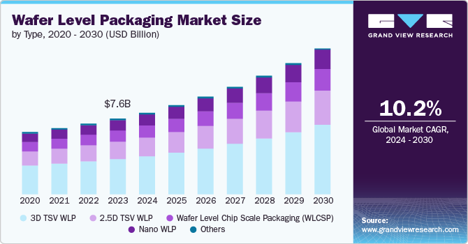
The global wafer level packaging market size was estimated at USD 7.56 billion in 2023 and is expected to grow at a CAGR of 10.2% from 2024 to 2030. Increasing demand for the technologically improved mobile devices and ongoing advancements in integrated circuits and semiconductor industry is expected to accelerate the growth of wafer layer packaging market during the forecast period.
In addition, rising demand for smaller and more compact electronic devices in established and emerging economies is shaping the dynamics of the wafer layer packaging market. Hence, as consumer electronics, automotive, and healthcare industries continue to demand smaller and more compact devices, wafer level packaging offers a solution by enabling the miniaturization of electronic components, leading to enhanced performance and functionality. For example, the rise of wearables such as smartwatches and fitness trackers has fueled the demand for wafer level packaging as it allows for the integration of multiple functions into a single compact chip.
Furthermore, the escalating adoption of Internet of Things (IoT) devices across various industries. The IoT ecosystem requires advanced packaging solutions to accommodate the diverse range of sensors, microcontrollers, and wireless communication modules in a compact form factor. Wafer level packaging facilitates the integration of multiple components onto a single chip, enabling the development of smaller, more power-efficient IoT devices. For instance, in the automotive sector, the proliferation of connected car technologies and advanced driver assistance systems (ADAS) has led to an increased need for wafer level packaging to enable the seamless integration of sensors and processors in a compact space.
Moreover, the continuous advancements in semiconductor technology, including the development of advanced packaging techniques such as fan-out wafer level packaging (FOWLP) and through-silicon vias (TSV), are driving the growth of the wafer level packaging market. These innovations have enabled increased functionality, improved performance, and reduced form factors, making wafer level packaging an attractive solution for manufacturers seeking to stay ahead in the competitive electronics market.
Type Insights
Based on type, the global wafer level packaging market has been segmented into 3D TSV WLP, 2.5D TSV WLP, Wafer Level Chip Scale Packaging (WLCSP), and Nano WLP. 3D Through-Silicon Via (TSV) Wafer Level Packaging (WLP) currently holds the majority of the total market share.it is a packaging technology that involves stacking multiple layers of chips vertically, allowing for enhanced capacity, decreased system space requirements, improved performance, and low power consumption. This segment is expected to contribute to rapid market expansion due to its technological advantages and efficiency.
2.5D Through-Silicon Via (TSV) Wafer Level Packaging (WLP) is widely used for its enhanced capacity, decreased system space requirements, improved performance, and low power consumption. This technology is utilized for devices such as microphones, pressure sensors, accelerometers, gyroscopes, capacitors, resistors, and transistors
Wafer Level Chip Scale Packaging (WLCSP) is currently the smallest available packaging technology in the market. It involves adding a protective layer of electronic connections and integrated circuits (ICs) at the wafer level.
Technology Insights
Based on the technology, the wafer level packaging market is segmented into Fan-in Wafer Level Packaging (FI-WLP) and Fan-out Wafer Level Packaging (FO-WLP). FI-WLP is known for its compact packaging suitable for small form factor applications, making it ideal for various devices such as microphones, pressure sensors, accelerometers, gyroscopes, capacitors, resistors, and transistors.
On the other hand, Fan-out Wafer Level Packaging (FO-WLP) is an enhancement of standard WLPs, enabling a greater number of I/O connections. This technology involves redistributing the I/Os beyond the chip area, enabling the integration of multiple chips within a single package. FO-WLP is seen as a low-cost advanced packaging alternative to packages that use silicon interposers, such as those seen in 2.5D and 3D packages.
End-use Insights
Based on the end use, the wafer level packaging market is segmented into consumer electronics, it & telecommunication, automotive, healthcare, and other end uses. Consumer electronics is a significant segment in the wafer level packaging market, registering highest revenue share of the market. The development of electronic packaging technology has led to the creation of extremely effective and reliable electrical connecting methods for electronic devices, contributing to the steady expansion of this segment.
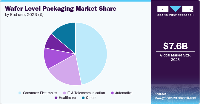
The IT & telecommunication segment is another important end use industry for wafer level packaging. This technology is crucial for meeting the high-performance demands of the telecommunications industry, driving manufacturers to scale performance, quality, capacity, and cost savings. In addition, the development of electronic packaging technology has led to the creation of reliable electrical connecting methods for electronic devices, which is beneficial for the IT & telecommunication sector.
Moreover, in the automotive industry, the use of wafers is expected to fuel the market growth during the forecast period. Wafer level packaging offers advantages such as structural support, clearance for high frequency operation, and mechanical protection, making it suitable for automotive applications. This technology is expected to contribute to the production of semiconductors with smaller, thinner, and lighter packages that meet the demands of the automotive industry.
Regional Insights
North American region has significant presence of leading semiconductor companies and advanced technological infrastructure contribute to its dominant position. Strong demand for advanced consumer electronics and high-performance computing devices. Substantial investments in R&D by major semiconductor firms. Favorable government policies supporting technological advancements.
Asia Pacific Wafer Level Packaging Market Trends
Asia Pacific dominated the market and accounted for the largest revenue share of over 52% in 2023. The region is particularly witnessing continuous advancements in packaging technologies, such as 3D wafer-level packaging and fan-out wafer-level packaging, are driving market growth across the region. The rising demand for miniaturized and high-performance electronic devices is propelling the adoption of wafer-level packaging solutions. Significant investments in research and development by major semiconductor companies are leading to innovations and cost-effective packaging solutions.
China wafer level packaging market is holds the highest market share in the Asia Pacific region. Its dominance is attributed to its vast semiconductor manufacturing industry and significant investments in advanced packaging technologies.
Rapid growth of consumer electronics and mobile devices market. Government initiatives promoting domestic semiconductor production. Presence of major semiconductor fabrication plants.
India wafer level packaging market is expected to register the fastest CAGR in the Asia Pacific region. The growth is fueled by increasing investments in the semiconductor sector and the rising demand for consumer electronics. Government initiatives like “Make in India” promoting local manufacturing. Growing demand for smartphones, tablets, and other electronic devices. Increasing focus on developing domestic semiconductor capabilities.
Europe Wafer Level Packaging Market Trends
Europe maintains a steady position in the global wafer-level packaging market. Key countries contributing to the market include Germany, France, and the UK, driven by the robust automotive and industrial sectors. Increasing adoption of IoT devices and smart technologies. Strong presence of automotive manufacturers integrating advanced semiconductor components. Supportive regulatory environment and funding for semiconductor research
Key Wafer Level Packaging Company Insights
The wafer level packaging (WLP) market is characterized by intense competition and rapid technological advancements. Companies are continuously investing in research and development to improve their WLP offerings, focusing on areas such as 3D integration, fan-out WLP, and advanced materials. Strategic partnerships and collaborations are common as firms seek to enhance their capabilities and expand their market presence.
-
In March 2024, Arizona State University (ASU) and Deca Technologies, a provider of advanced wafer- and panel-level packaging technology, announced a collaboration to create North America's first fan-out wafer-level packaging (FOWLP) research and development center. This partnership aims to accelerate innovation and bolster U.S. technology leadership in the semiconductor industry.
-
In March 2024, Taiwan Semiconductor Manufacturing Company Limited planned to expand its advanced chip packaging capacity in Japan. This strategic move is part of company’s efforts to enhance its global manufacturing capabilities and meet the growing demand for advanced semiconductor packaging technologies.
-
In June 2023, Onto Innovation launched an Applications Center of Excellence focused on panel-level packaging (PLP) at its Wilmington, Massachusetts headquarters. The facility was expected to provide customers with hands-on experience and access to company’s hardware and software solutions, as well as systems and processes from partnering OEMs and materials providers. This collaborative approach aims to help customers accelerate their technology roadmaps and shorten time to yield when in production, particularly for advanced packaging processes such as PLP, advanced IC substrates (AICS), and wafer-level packaging.
Key Wafer Level Packaging Companies:
The following are the leading companies in the wafer level packaging market. These companies collectively hold the largest market share and dictate industry trends.
- Amkor Technology
- Taiwan Semiconductor Manufacturing Company Limited
- MKS Instruments
- SMTA
- MueTec
- ULVAC
- Micross
- Nanotronics
- JCET
- ECI Technology
- KLA Corporation
- Bruker
- CAPLINQ Corporation
- Nordson Corporation
- ASE
Wafer Level Packaging Market Report Scope
Report Attribute
Details
Market size value in 2024
USD 8.12 billion
Revenue forecast in 2030
USD 14.55 billion
Growth rate
CAGR of 10.2% from 2024 to 2030
Historical data
2018 - 2022
Forecast period
2024 - 2030
Quantitative units
Revenue in USD million, and CAGR from 2024 to 2030
Report coverage
Revenue forecast, competitive landscape, growth factors and trends
Segments covered
Type, technology, end-use, region
Regional scope
North America; Europe; Asia Pacific; Central & South America; Middle East & Africa
Country Scope
U.S.; Canada; Mexico; Germany; France; UK; Italy; Spain; China; India; Japan; South Korea; Australia; Brazil; Argentina; Saudi Arabia; South Africa; UAE
Key companies profiled
Amkor Technology; Taiwan Semiconductor Manufacturing Company Limited; MKS Instruments; SMTA; MueTec; ULVAC; Micross; Nanotronics; JCET; ECI Technology; KLA Corporation; Bruker; CAPLINQ Corporation; Nordson Corporation; ASE
Customization scope
Free report customization (equivalent up to 8 analyst’s working days) with purchase. Addition or alteration to country, regional & segment scope
Pricing and purchase options
Avail customized purchase options to meet your exact research needs. Explore purchase options
Global Wafer Level Packaging Market Report Segmentation
This report forecasts revenue growth at global, regional, and country levels and provides an analysis of the latest industry trends in each of the sub-segments from 2018 to 2030. For the purpose of this study, Grand View Research has segmented the wafer level packaging market report on the basis of type, technology, end-use, and region:
-
Type Outlook (Revenue, USD Million, 2018 - 2030)
-
3D TSV WLP
-
2.5D TSV WLP
-
Wafer Level Chip Scale Packaging (WLCSP)
-
Nano WLP
-
Others
-
-
Technology Outlook (Revenue, USD Million, 2018 - 2030)
-
Fan-in Wafer Level Packaging (FI-WLP)
-
Fan-out Wafer Level Packaging (FO-WLP)
-
-
End-use Outlook (Revenue, USD Million, 2018 - 2030)
-
Consumer Electronics
-
IT & Telecommunication
-
Automotive
-
Healthcare
-
Others
-
-
Regional Outlook (Revenue, USD Million, 2018 - 2030)
-
North America
-
U.S.
-
Canada
-
Mexico
-
-
Europe
-
Germany
-
UK
-
France
-
Italy
-
Spain
-
-
Asia Pacific
-
China
-
India
-
Japan
-
South Korea
-
Australia
-
-
Central & South America
-
Brazil
-
Argentina
-
-
Middle East & Africa
-
Saudi Arabia
-
UAE
-
South Africa
-
-
Frequently Asked Questions About This Report
b. The global wafer level packaging market size was estimated at USD 7.56 billion in 2023 and is expected to reach USD 8.12 billion in 2024.
b. The wafer level packaging market is expected to grow at a compound annual growth rate of 10.2% from 2024 to 2030, reaching USD 14.55 billion by 2030.
b. Based on the technology, the wafer level packaging market is segmented into Fan-in Wafer Level Packaging (FI-WLP) and Fan-out Wafer Level Packaging (FO-WLP). FI-WLP is known for its compact packaging, suitable for small form factor applications, making it ideal for various devices such as microphones, pressure sensors, accelerometers, gyroscopes, capacitors, resistors, and transistors.
b. Key players in the market include Amkor Technology, Taiwan Semiconductor Manufacturing Company Limited, MKS Instruments, SMTA, MueTec, ULVAC, Macross, Nanotronics, JCET, ECI Technology, KLA Corporation, Bruker, CAPLINQ Corporation, Nordson Corporation; and ASE.
b. Increasing demand for technologically improved mobile devices and ongoing advancements in integrated circuits and the semiconductor industry are expected to accelerate the growth of the wafer layer packaging market during the forecast period.
Share this report with your colleague or friend.
![gvr icn]()
NEED A CUSTOM REPORT?
We can customize every report - free of charge - including purchasing stand-alone sections or country-level reports, as well as offer affordable discounts for start-ups & universities. Contact us now
![Certified Icon]()
We are GDPR and CCPA compliant! Your transaction & personal information is safe and secure. For more details, please read our privacy policy.
We are committed towards customer satisfaction, and quality service.
"The quality of research they have done for us has been excellent."
