- Home
- »
- Plastics, Polymers & Resins
- »
-
Semiconductor Packaging Market Size & Share Report, 2030GVR Report cover
![Semiconductor Packaging Market Size, Share & Trends Report]()
Semiconductor Packaging Market (2025 - 2030) Size, Share & Trends Analysis Report By Material (Organic Substrate, Bonding Wire, Encapsulation Resins, Die Attach Material, Ceramic Packages), By Packaging Technology, By End-use, By Region, And Segment Forecasts
- Report ID: GVR-4-68040-338-4
- Number of Report Pages: 220
- Format: PDF
- Historical Range: 2018 - 2023
- Forecast Period: 2024 - 2030
- Industry: Bulk Chemicals
- Report Summary
- Table of Contents
- Segmentation
- Methodology
- Download FREE Sample
-
Download Sample Report
Semiconductor Packaging Market Summary
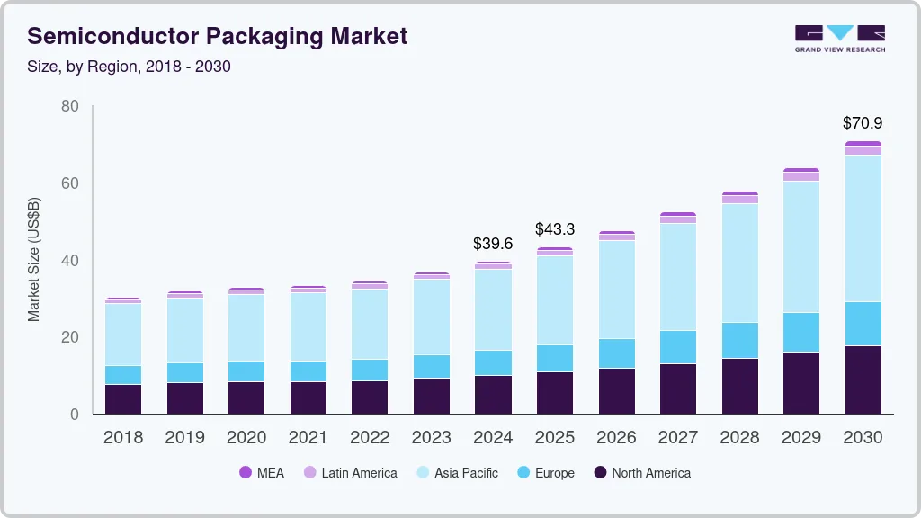
The global semiconductor packaging market size was estimated at USD 39,585.2 million in 2024 and is projected to reach USD 70,896.4 billion by 2030, growing at a CAGR of 10.4% from 2025 to 2030. With the proliferation of smartphones, tablets, and other consumer electronics, the need for advanced semiconductor packaging is rising.
Key Market Trends & Insights
- Asia Pacific semiconductor packaging market holds the largest market share of over 53% in 2023.
- The semiconductor packaging market of China leads the Asia Pacific industry.
- By material, organic substrate dominated the overall market with a market share of over 41.5% in 2023.
- By packaging technology, the traditional packaging segment dominated the market and accounted for the largest revenue share of over 52.5% in 2023..
- By end-use, consumer electronics end user segment dominated market and accounted for largest revenue share of over 43.8% in 2023..
Market Size & Forecast
- 2024 Market Size: USD 39,585.2 Million
- 2030 Projected Market Size: USD 70,896.4 Million
- CAGR (2025-2030): 10.4%
- Asia Pacific: Largest market in 2023
The automotive industry's shift towards electric vehicles (EVs) and autonomous driving technologies necessitates sophisticated semiconductor packaging to handle higher performance and reliability standards. Companies like TSMC and Intel are investing heavily in automotive-grade semiconductor solutions. The growing adoption of Artificial Intelligence (AI) and the Internet of Things (IoT) is fueling the demand for advanced packaging technologies. These technologies require high integration levels and efficient heat dissipation, driving innovations in packaging solutions like Fan-Out Wafer Level Packaging (FO-WLP) and System-in-Package (SiP).
The trend towards miniaturization in electronics is driving the need for smaller, more efficient packaging solutions. This demand is boosting the adoption of 3D packaging technologies that allow more functionalities to be packed into smaller spaces. The development of new materials such as organic substrates and advanced encapsulation resins is creating opportunities for more efficient and durable packaging solutions. For instance, in 2023, Amkor Technology launched new advanced substrate materials that enhance thermal performance and reliability.
Material Insights
Organic substrate dominated the overall market with a market share of over 41.5% in 2023 and is expected to witness robust growth over the forecast period. Organic substrates are widely used due to their cost-effectiveness and excellent electrical performance. They dominate the market and are driven by high demand from consumer electronics and communication industries.
Bonding wire is essential for connecting the semiconductor die to the package, is witnessing rapid growth. The shift towards finer and more efficient wires, especially in advanced packaging, is propelling this segment. Ceramic packages offer high thermal conductivity and are used in high-performance applications, such as aerospace and defense. They are favored for their reliability in harsh environments. Die Attach materials are essential for bonding semiconductor dies to substrates. Advances in materials with better thermal and electrical conductivity are driving this segment.
Packaging Technology Insights
The traditional packaging segment dominated the market and accounted for the largest revenue share of over 52.5% in 2023. Based on the packaging technology, the market is segmented into advanced packaging and traditional packaging. Traditional packaging, including leadframe-based and wire bonding, holds the largest market share due to its extensive use in consumer electronics and automotive sectors. Its cost-effectiveness and established manufacturing processes make it a preferred choice.
On the other hand, advanced packaging segment is expected to witness robust growth with a CAGR of 12.3% over the forecast period. Advanced packaging technologies like Flip Chip, System-in-Package (SiP), and 3D/5D packaging are growing rapidly due to their ability to enhance device performance and reduce size. These technologies are crucial for high-demand sectors like AI and IoT.
End-use Insights
Consumer electronics end user segment dominated market and accounted for largest revenue share of over 43.8% in 2023. Consumer Electronics segment dominates the market due to the high volume of semiconductor use in devices like smartphones, tablets, and wearables. The trend towards miniaturization and multifunctional devices drives the demand for advanced packaging.
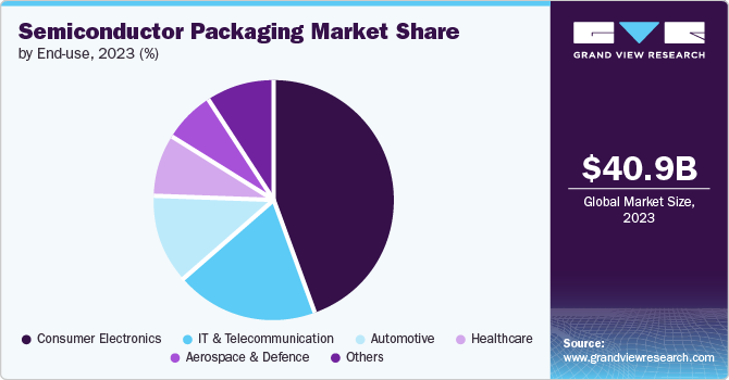
On the other hand, the aerospace & defense end user segment is expected to grow at the fastest CAGR of 11.4% during the forecast period. The aerospace and defense sector requires robust and reliable packaging solutions for harsh environments. The need for advanced, high-reliability packages is driving the fastest growth in this segment.
The transition to electric and autonomous vehicles is increasing the need for reliable and high-performance semiconductor packaging. This sector is experiencing substantial growth in demand for advanced packaging technologies. With the rise of medical devices and diagnostics, the healthcare sector is increasingly relying on advanced semiconductor packaging for reliable and compact solutions.
Regional Insights
North America semiconductor packaging market is projected to gain significant numbers of shares in the upcoming years. The U.S. holds the highest market share in the North American market due to its advanced technological infrastructure, significant investments in R&D, and a robust ecosystem of semiconductor companies. The country is home to major semiconductor giants like Intel, Qualcomm, and Texas Instruments, which continuously drive innovation in packaging technologies. The U.S. government's CHIPS Act, which provides substantial funding for domestic semiconductor manufacturing and packaging, is a significant driver of market growth. This act is designed to reduce dependency on foreign semiconductor suppliers and bolster the domestic semiconductor industry.
U.S. Semiconductor Packaging Market Trends
The semiconductor packaging market of U.S. is leading owing to the AI and 5G technology development. Companies like NVIDIA and Qualcomm are at the forefront of integrating advanced packaging solutions to meet the demands of these high-growth sectors. For instance, Qualcomm's advancements in 5G modem packaging are crucial in maintaining its competitive edge in the telecommunications market. Intel's investment in expanding its advanced packaging capabilities is a prime example. In 2023, Intel announced a significant expansion of its semiconductor packaging facility in Arizona, aiming to increase the production of advanced packaging technologies like EMIB (Embedded Multi-Die Interconnect Bridge) and Foveros.
Asia Pacific Semiconductor Packaging Market Trends
Asia Pacific semiconductor packaging market holds the largest market share of over 53% in 2023 and exhibits the fastest growth in the semiconductor packaging market. This growth is fueled by the region's dominant electronics manufacturing base, increasing investments in semiconductor technologies, and rapid technological advancements. Major Chinese firms like Taiwan Semiconductor Manufacturing Company have expanded their packaging facilities in China to cater to the growing demand for advanced semiconductor solutions. TSMC’s new plant in Nanjing, focusing on advanced packaging and testing services, highlights this expansion.
The semiconductor packaging market of China leads the Asia Pacific industry due to its expansive electronics manufacturing industry and significant government support for semiconductor development. Chinese companies are rapidly advancing in semiconductor packaging technologies to reduce reliance on imports and enhance their global competitiveness. The Chinese government's "Made in China 2025" initiative aims to transform the country into a global leader in advanced technologies, including semiconductor packaging. Investments in domestic semiconductor companies, such as Semiconductor Manufacturing International Corporation (SMIC), are a testament to this commitment.
India semiconductor packaging market is experiencing a significant growth rate in the Asia Pacific region. The country’s burgeoning electronics manufacturing sector and supportive government policies are key drivers of this rapid expansion. The Indian government has launched several incentive programs, such as the Production Linked Incentive (PLI) scheme, to attract investment in semiconductor manufacturing and packaging. This has led to increased investment from both domestic and international companies. Recent announcements, such as Vedanta and Foxconn's joint venture to establish a semiconductor fabrication plant in Gujarat, underscore India's growing capabilities in the semiconductor industry. These developments are set to boost the demand for advanced packaging solutions significantly.
Europe Semiconductor Packaging Market Trends
The semiconductor packaging market of Europe is majorly dominated by Germany which can be attributed to its strong automotive and industrial sectors, which are major consumers of advanced semiconductor technologies. German companies are leaders in developing cutting-edge automotive electronics and industrial automation systems that rely heavily on advanced semiconductor packaging. European companies is actively involved in collaborative research programs that focus on semiconductor technology advancements. For instance, the European Union’s Horizon Europe program supports various German initiatives aimed at developing next-generation semiconductor packaging technologies.
Germany semiconductor packaging market is mainly driven by the automotive industry. Companies like Bosch and Infineon are heavily investing in advanced packaging technologies for electric vehicles (EVs) and autonomous driving systems. For example, Infineon has expanded its chip packaging capabilities in Dresden to cater to the increasing demand for EV components. Germany's push towards Industry 4.0 is accelerating the adoption of advanced semiconductor solutions. The focus on smart manufacturing and automation is driving the need for robustness and reliablility.
Key Semiconductor Packaging Company Insights
The market is fragmented with the presence of a significant number of companies. Semiconductor packaging industry has been witnessing a significant number of new product launches, mergers & acquisitions, and expansions over the past few years. This can be attributed to the circular economy initiatives and innovation in materials.
Key Semiconductor Packaging Companies:
The following are the leading companies in the semiconductor packaging market. These companies collectively hold the largest market share and dictate industry trends.
- ASE
- Amkor Technology
- JCET Group
- Siliconware Precision Industries Co. Ltd.
- Powertech Technology Inc.
- Tianshui Huatian Technology Co. Ltd
- Fujitsu Semiconductor Ltd
- UTAC
- ChipMOS TECHNOLOGIES INC.
- CHIPBOND Technology Corporation
- Intel Corporation
- Samsung
- Unisem (M) Berhad
- Camtek
- LG Chem
Recent Developments
-
In March 2024, the U.S. Department of Commerce and Intel Corporation signed a USD non-binding preliminary memorandum of terms (PMT). Under these terms, USD 8.5 billion direct funding will be provided to Intel Corporation for its commercial semiconductor projects under the CHIPS and Science Act, thus driving demand for semiconductor packaging.
-
In March 2024, Taiwan based Taiwan Semiconductor Manufacturing Company Limited announced its intent to construct an advanced packaging facility in Japan for semiconductors. The company is planning to introduce its chip on wafer on substrate (CoWoS) packaging technology in Japan that involves stacking chips on top of each other. This packaging helps in boosting processing power and reducing power consumption in semiconductor chips.
-
In November 2023, JCET Automotive Electronics (Shanghai) Co., Ltd, the holding company of Jiangsu Changdian Technology Co., Ltd. is expected to receive an investment of USD 0.60 billion (CNY 4.4 billion) for the construction of construction of advanced packaging facility for automotive chip products in the Lingang Special Area of Shanghai.
-
In September 2023, Intel Corporation, launched a glass substrate for next-generation advanced packaging. The glass substrate exhibits properties such as better mechanical and thermal stability and ultra-low flatness, which increases the interconnect density in a substrate. These features of glass substrate help in the production of high-performance, high-density chip packages suitable for data-intensive workloads.
Semiconductor Packaging Market Report Scope
Report Attribute
Details
Market size value in 2025
USD 43301.4 million
Revenue forecast in 2030
USD 70,896.4 million
Growth rate
CAGR of 10.4% from 2025 to 2030
Actual data
2018 - 2023
Forecast period
2025 - 2030
Quantitative units
Revenue in USD million/billion, and CAGR from 2025 to 2030
Report coverage
Revenue forecast, competitive landscape, growth factors and trends
Segments covered
Material, technology, end-use, region
Regional scope
North America; Europe; Asia Pacific; Central & South America; Middle East & Africa
Country Scope
U.S.; Canada; Mexico; Germany; France; UK; Italy; Spain; China; India; Japan; South Korea; Brazil; Argentina; Israel; South Africa; UAE
Key companies profiled
ASE; Amkor Technology; JCET Group; Siliconware Precision Industries Co. Ltd.; Powertech Technology Inc.; Tianshui Huatian Technology Co. Ltd; Fujitsu Semiconductor Ltd; UTAC; ChipMOS TECHNOLOGIES INC.; CHIPBOND Technology Corporation; Intel Corporation; Samsung; Unisem (M) Berhad; Camtek; LG Chem
Customization scope
Free report customization (equivalent up to 8 analyst’s working days) with purchase. Addition or alteration to country, regional & segment scope
Pricing and purchase options
Avail customized purchase options to meet your exact research needs. Explore purchase options
Global Semiconductor Packaging Market Report Segmentation
This report forecasts revenue growth at global, regional, and country levels and provides an analysis of the latest industry trends in each of the sub-segments from 2018 to 2030. For this study, Grand View Research has segmented the global semiconductor packaging market report based on material, technology, end-use, and region:
-
Material Outlook (Revenue, USD Million, 2018 - 2030)
-
Organic Substrate
-
Bonding Wire
-
Leadframes
-
Encapsulation Resins
-
Ceramic Package
-
Die Attach Material
-
Thermal Interface Materials
-
Solder Balls
-
Others
-
-
Technology Outlook (Revenue, USD Million, 2018 - 2030)
-
Advanced Packaging
-
Flip Chip
-
SIP
-
5D/3D
-
Embedded Die
-
Fan-in Wafer Level Packaging (FI-WLP)
-
Fan-out Wafer Level Packaging (FO-WLP)
-
-
Traditional Packaging
-
-
End-use Outlook (Revenue, USD Million, 2018 - 2030)
-
Consumer Electronics
-
Automotive
-
Healthcare
-
IT & Telecommunication
-
Aerospace & Defence
-
Others
-
-
Regional Outlook (Revenue, USD Million, 2018 - 2030)
-
North America
-
U.S.
-
Canada
-
Mexico
-
-
Europe
-
Germany
-
UK
-
France
-
Italy
-
Spain
-
-
Asia Pacific
-
China
-
India
-
Japan
-
South Korea
-
-
Central & South America
-
Brazil
-
Argentina
-
-
Middle East & Africa
-
Israel
-
UAE
-
South Africa
-
-
Frequently Asked Questions About This Report
b. The global semiconductor packaging packaging market size was estimated at USD 40.91 billion in 2023 and is expected to reach USD 43.95 billion in 2024.
b. The global semiconductor packaging market is expected to grow at a compound annual growth rate of 10.2% from 2024 to 2030, reaching USD 78.72 billion by 2030.
b. Organic substrates dominated the overall market with a market share of over 41.5% in 2023 and are expected to witness robust growth with a CAGR of 10.7% over the forecast period. They are widely used due to their cost-effectiveness and excellent electrical performance. The market is driven by high demand from consumer electronics and communication industries.
b. Key Players in the market include ASE, Amkor Technology, JCET Group, Siliconware Precision Industries Co. Ltd., Powertech Technology Inc., Tianshui Huatian Technology Co. Ltd, Fujitsu Semiconductor Ltd, UTAC, ChipMOS TECHNOLOGIES INC., CHIPBOND Technology Corporation, Intel Corporation, Samsung, Unisem (M) Berhad, Camtek, and LG Chem.
b. The global semiconductor packaging market is expected to increase rapidly as the demand for smartphones, tablets, and other consumer electronics rises, as does the need for advanced semiconductor packaging. These devices require compact and efficient packaging solutions that ensure high performance and reliability.
Share this report with your colleague or friend.
Need a Tailored Report?
Customize this report to your needs — add regions, segments, or data points, with 20% free customization.

ISO 9001:2015 & 27001:2022 Certified
We are GDPR and CCPA compliant! Your transaction & personal information is safe and secure. For more details, please read our privacy policy.
Trusted market insights - try a free sample
See how our reports are structured and why industry leaders rely on Grand View Research. Get a free sample or ask us to tailor this report to your needs.


