- Home
- »
- Advanced Interior Materials
- »
-
Semiconductor Chemical Vapor Deposition Equipment Market Report, 2030GVR Report cover
![Semiconductor Chemical Vapor Deposition Equipment Market Size, Share & Trends Report]()
Semiconductor Chemical Vapor Deposition Equipment Market Size, Share & Trends Analysis Report By Product Type (Atmospheric-Pressure Chemical Vapor Deposition, Low-Pressure Chemical Vapor Deposition), By Application, By Region, And Segment Forecasts, 2024 - 2030
- Report ID: GVR-4-68040-294-3
- Number of Report Pages: 152
- Format: PDF, Horizon Databook
- Historical Range: 2018 - 2023
- Forecast Period: 2024 - 2030
- Industry: Advanced Materials
Market Size & Trends
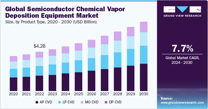
The global semiconductor chemical vapor deposition equipment market size was estimated at USD 4.5 billion in 2023 and is anticipated to grow at a CAGR of 7.7% from 2024 to 2030. High demand for electronic devices, such as smartphones, tablets, laptops, and IoT devices, directly impacts semiconductor production. Therefore, increased demand for these devices can lead to higher demand for semiconductor Chemical Vapor Deposition (CVD) equipment. Moreover, disruptions in global supply chain, such as shortage of critical semiconductor components, can influence equipment demand as manufacturers seek to secure their supply chains and reduce vulnerabilities. This, in turn, is likely to increase demand for semiconductor CVD equipment over the forecast period.
The demand for semiconductors is increasing worldwide as the design of integrated circuits (ICs) is becoming increasingly complicated, resulting in the use of many semiconductors for developing them. Semiconductors are used to develop ICs as they help minimize production costs, reduce time required for mass production, and enhance value of final products in terms of operations. Thus, rising demand for semiconductors is anticipated to positively impact the semiconductor chemical vapor deposition equipment market over the forecast period.
In addition, companies in the semiconductor market space have announced hundreds of projects to enhance their manufacturing capacity in the U.S. owing to the implementation of the Chips Act in 2020. Thus, increasing investment in the semiconductor industry coupled with rising semiconductor equipment facilities is anticipated to propel the demand for semiconductor chemical vapor deposition equipment. For instance, in March 2023, Samsung Electronics announced to invest USD 228 billion in an advanced semiconductor facility in South Korea.
According to the Semiconductor Industry Association, Taiwan, South Korea, Japan, and China accounted for 72% of global semiconductor production in 2022 with its previous manufacturing hubs, such as the U.S. and Japan, focusing on the highly profitable countries for exporting their products. Moreover, as of 2022, Asia Pacific was the largest semiconductor market with China being the largest consumer of semiconductors.
In December 2022, Taiwan Semiconducting Manufacturing Co. announced an increase in investments to enhance its manufacturing capacity in the U.S., signaling a shift in geographic dynamics. Economic nationalism and/or supply chain security policies in Japan, South Korea, and India are anticipated to further alter the manufacturing environment with an increased number of countries attempting to boost onshore production of semiconductors and minimize their reliance on supplies from Taiwan.
Market Concentration & Characteristics
The industry growth stage is medium, and its pace is accelerating. It is characterized by a high degree of innovation, which can be attributed to rapid technological advancements. Moreover, market players are adopting organic and inorganic growth strategies, such as product launches, geographical expansions, mergers & acquisitions, and collaborations, to strengthen their global market position.
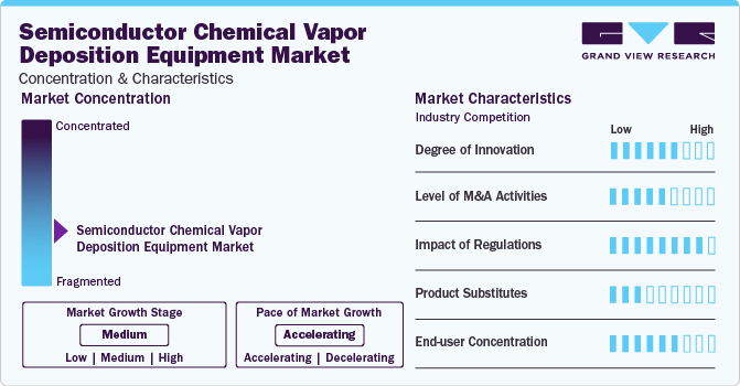
Regulations play a crucial role in shaping the semiconductor industry, particularly with respect to chemical vapor deposition (CVD) equipment. As CVD processes involve the use of hazardous chemicals and high-temperature operations, stringent regulations are imposed to ensure worker safety, environmental protection, and product quality. Compliance with Occupational Safety and Health Administration (OSHA) standards, Environmental Protection Agency (EPA) guidelines, and international directives like REACH (Registration, Evaluation, Authorization, and Restriction of Chemicals) requires significant investments in equipment design, manufacturing processes, and operational protocols.
Degree of innovation is pivotal in driving technological advancements and market competitiveness. Innovations in CVD equipment are fueled by various factors, including demand for higher performance, increased functionality, reduced costs, and environmental sustainability. Semiconductor manufacturers strive to enhance deposition processes, deposition uniformity, film quality, and throughput while minimizing energy consumption and waste generation. Key areas of innovation include novel reactor designs, advanced process control systems, precise precursor delivery mechanisms, and deposition techniques tailored for specific applications such as atomic layer deposition (ALD) and plasma-enhanced CVD (PECVD).
End-user concentration significantly influences industry dynamics, innovation trends, and market strategies. End-user concentration refers to the distribution of semiconductor device manufacturers and other industries that utilize CVD equipment for thin-film deposition. In a highly concentrated market, a few large companies dictate the demand for CVD equipment, exerting considerable influence on technology adoption, price negotiations, and product specifications.
Presence and viability of potential substitutes in influence industry dynamics, innovation strategies, and market positioning. Substitutes are alternative technologies or methods that can achieve similar outcomes to CVD equipment in thin-film deposition. Availability and attractiveness of substitutes can impact the demand for CVD equipment and shape supplier competitiveness.
Product Type Insights
The Atmospheric-Pressure Chemical Vapor Deposition (AP CVD) product segment held the largest revenue share in 2023. AP CVD operates at atmospheric pressure, eliminating the need for vacuum chambers or costly vacuum pumps required in traditional CVD processes. This reduces equipment complexity and lowers capital expenditures for semiconductor manufacturers, making AP CVD an attractive option for mass production.
The demand for low-pressure chemical vapor deposition (LP CVD) is expected to grow at a significant CAGR from 2023 to 2030 in terms of revenue. The low-pressure environment in LP CVD minimizes gas-phase reactions and impurity incorporation during film deposition, resulting in high-purity films suitable for sensitive semiconductor applications. This capability is particularly essential for depositing epitaxial layers and other critical semiconductor materials where impurities can significantly impact device performance and reliability.
Application Insights
The analog chips application segment held the largest share and accounted for 42.0% of the market in 2023. Analog chips often include semiconductor devices, such as bipolar junction transistors (BJTs) and metal-oxide-semiconductor field-effect transistors (MOSFETs), fabricated using thin film deposition techniques. CVD processes allow deposition of semiconducting materials, such as silicon (Si) and compound semiconductors (e.g., gallium arsenide or GaAs), with controlled doping profiles and crystal structures necessary for achieving desired device characteristics and performance parameters.
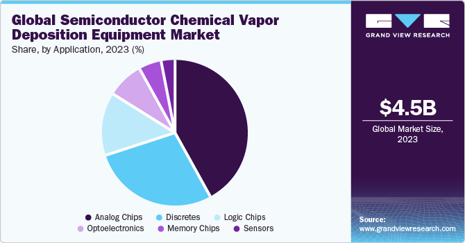
The memory chip application segment is projected to grow at a significant CAGR. Memory chip fabrication often involves depositing liner and barrier layers to prevent diffusion of metals and contaminants, enhancing adhesion between different materials, and improving device reliability. CVD processes enable the deposition of conformal and uniform liner/barrier films made of titanium nitride (TiN) and tantalum nitride (TaN), ensuring optimal device performance and longevity.
Regional Insights
The semiconductor chemical vapor deposition equipment market in North America is expected to witness growth over the forecast period. The semiconductor manufacturing equipment market in North America forms an integral part of the global semiconductors industry. U.S., Canada, and Mexico have several prominent semiconductor companies, research organizations, and manufacturing facilities. Semiconductors industry is also characterized by rapid technological developments, with semiconductor devices becoming increasingly powerful and energy efficient.
U.S. Semiconductor Chemical Vapor Deposition Equipment Market Trends
The semiconductor chemical vapor deposition equipment market in the U.S. is expected to grow at a considerable CAGR from 2024 to 2030. The U.S.-based semiconductor equipment manufacturers continually invest in research and development activities to launch innovative tools for advanced packaging, lithography, metrology, and process control.
The Canada semiconductor chemical vapor deposition equipment market is expected to register high growth over the forecast period. The semiconductor manufacturing equipment market in Canada plays a vital role in supporting the growing technology sector and semiconductors industry. One significant trend in Canada is a strong emphasis on research and development (R&D) activities and innovations.
Asia Pacific Semiconductor Chemical Vapor Deposition Equipment Market Trends
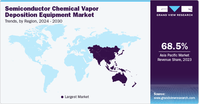
The semiconductor chemical vapor deposition equipment market in Asia Pacificdominated the global market and accounted for a revenue share of 68.5% in 2023. The governments have played a pivotal role, offering a list of investments that are in the pipeline. For instance, companies in Taiwan plan to invest over USD 107 billion in semiconductor production by 2025. Japan has also set up a fund of JPY200 billion to attract investment in advanced technology and promote R&D. Japan eventually plans to expand its existing policies targeting the semiconductor industry.
The semiconductor chemical vapor deposition equipment market in China is estimated to grow at a significant CAGR over the forecast period. China has been striving to achieve self-dependency in semiconductors. For this, in August 2023, it launched a new investment fund from the National Integrated Circuit Industry Investment Fund Co., known as the Big Fund. It aims to raise USD 40 billion with semiconductor manufacturing equipment as an important investment area. This decision was made in response to sanctions imposed by the U.S. on China in August 2022 for their advanced semiconductor manufacturing equipment. Japan and the Netherlands followed the U.S. by taking similar steps.
The India semiconductor chemical vapor deposition equipment market is expected to grow at a CAGR of over 8% from 2024 to 2030. India continued its foray into the semiconductor business in 2023 and is striving to become one of the largest global producers catering to critical applications and high-volume automotive industry.
Europe Semiconductor Chemical Vapor Deposition Equipment Market Trends
The semiconductor chemical vapor deposition equipment market in Europe is anticipated to witness significant growth from 2024 to 2030. Substantial efforts are being taken to secure semiconductor industry’s supply chain by the EU, which is introducing a host of policy measures. For instance, in February 2022, the European Commission commenced a formal evaluation of the "EU CHIPS Act". This Act offers targeted support of up to USD 43 billion for Europe's semiconductor industry.
The Germany semiconductor chemical vapor deposition equipment market is expected to grow at a significant CAGR over the forecast period. Germany has been making strides in semiconductor manufacturing in order to address supply chain risk and excessive dependence on imports from South Korea and Taiwan. In July 2023, the EU adopted the CHIPS Act, a USD 45.73 billion subsidy plan, to double its chip-making capacity by 2030. This Act aims to address vulnerabilities and dependencies on foreign players.
The semiconductor chemical vapor deposition equipment market in the UK held a sizeable share of Europe in 2023, owing to substantial government efforts. In January 2023, the UK government announced that it would provide direct taxpayer funding to support domestic semiconductor manufacturers to promote domestic production and curtail excessive imports. In May 2023, Britain announced a USD 1.23 billion investment to promote new semiconductor manufacturing for developing a USD 1.23 trillion industry in the next 10 years.
Central & South America Semiconductor Chemical Vapor Deposition Equipment Market Trends
The semiconductor chemical vapor deposition equipment market in Central & South America is estimated to grow rapidly over the forecast period, owing to high potential for growth and development within the global semiconductor industry. One key trend is the increasing demand for semiconductor manufacturing equipment due to the growing technology sector in several countries across Central & South America.
Middle East & Africa Semiconductor Chemical Vapor Deposition Equipment Market Trends
The semiconductor chemical vapor deposition equipment market in the Middle East & Africa is experiencing rapid development due to ongoing industrialization and urbanization, resulting in an increased demand for semiconductor-based products in advanced machinery, computers, and consumer goods. As a result, these countries are trying to set up semiconductor manufacturing units in the region, leading to new growth opportunities for semiconductor equipment manufacturers.
Key Semiconductor Chemical Vapor Deposition Equipment Company Insights
The market is fragmented, with various global and regional product manufacturers introducing innovative systems and technologies. Various industry participants' strategies typically involve new product development, product upgrades, and expansions to boost market penetration and respond to the changing technical needs of various application industries. Major players form technical partnerships to innovate and develop novel product lines, therefore expanding their consumer base. In addition, evolving consumer preferences, quality requirements, and energy efficiency are projected to offer new opportunities for key participants in the coming years.
A few key players operating in the semiconductor CVD equipment market include, KLA Corporation, Lam Research Corporation, and Applied Materials Inc.
-
Applied Materials Inc. operates in three business segments namely Semiconductor systems, applied global services (AGS), display, and adjacent markets. The semiconductor systems market develops, manufactures, and sells a diverse range of manufacturing equipment used to fabricate semiconductor chips, termed ICs.
-
Lam Research Corporation is a U.S.-based wafer fabrication equipment manufacturer and related service provider in the semiconductor industry. It designs and builds products in front-end wafer processing, including equipment for thin-film deposition, photoresist strips, and plasma etch.
Tokyo Electron Limited; Blue Wave Semi; PhotonExport; and Vivid Inc., are some of the emerging players in the market.
-
Tokyo Electron Limited is a Japanese electronics and semiconductor company. The company manufactures products for four sequential key processes necessary for semiconductor scaling: Deposition, coater, etch, and cleaning.
-
Blue Wave Semiconductors is a provider of advanced semiconductor vapor deposition equipment, specializing in innovative solutions for semiconductor manufacturing. With a focus on research and development, the company offers cutting-edge technologies to enable production of high-performance semiconductor devices.
Key Semiconductor Chemical Vapor Deposition Equipment Companies:
The following are the leading companies in the semiconductor chemical vapor deposition equipment market. These companies collectively hold the largest market share and dictate industry trends.
- Aixtron Se
- Applied Materials, Inc.
- Asm International
- Cvd Equipment Corporation
- Oxford Instruments Plc
- Lam Research Corporation
- Tokyo Electron Limited
- Ulvac Inc.
- Veeco Instruments Inc.
- KLA Corporation
- HORIBA
- NBM Design.
- Blue Wave Semi
- PhotonExport
- Vivid Inc.
Recent Developments
-
In September 2023, Gallium Semiconductor introduced the GTH2e-2425300P ISM CW amplifier. This amplifier operates in the 2.4-2.5GHz range and delivers 300W of power. It features pre-matched discrete GaN-on-SiC High Electron Mobility Transistor (HEMT) technology, offering enhanced efficiency suitable for various industrial, scientific, and medical (ISM) applications. These include semiconductor plasma sources and microwave plasma chemical vapor deposition (MPCVD) equipment utilized in synthetic diamond production, among others.
-
In May 2023, FUJIFILM Corporation acquired semiconductor high purity process chemicals (HPPC) business of KMG Corporation (KMG) for USD 700 million. This allows Fujifilm to expand its portfolio of electronic chemicals and services, leveraging KMG's expertise. Specifically, the acquisition encompasses KMG's line of HPPCs, which play a vital role in etching and cleaning of silicon wafers used in semiconductor manufacturing. This segment of materials is experiencing significant growth, and by integrating KMG's capabilities, Fujifilm aims to better serve its customers' evolving needs in the semiconductor production landscape.
-
In October 2021, Oxford Instruments and its research partner Industrial Technology Research Institute (ITRI) unveiled groundbreaking technological advancements to significantly benefit crucial hyper-growth sectors like electric vehicles, data centers, and 5G networks. These advancements can allow critical transistor components to operate at higher voltages. This improvement not only enhances performance and reliability but also enables safer and more energy-efficient operation, particularly in 'E-mode' state, compared to previous devices. This innovative technology, known as GaN MISHEMT, introduces a novel device architecture for Gallium Nitride (GaN) High Electron Mobility Transistors (HEMTs). This architecture features a recessed and insulated gate connection within AlGaN layer, offering enhanced functionality and performance characteristics.
Semiconductor Chemical Vapor Deposition Equipment Market Report Scope
Report Attribute
Details
Market size value in 2024
USD 4.80 billion
Revenue forecast in 2030
USD 7.50 billion
Growth rate
CAGR of 7.7% from 2024 to 2030
Historical data
2018 - 2023
Forecast period
2024 - 2030
Quantitative units
Revenue in USD million/billion and CAGR from 2024 to 2030
Report coverage
Revenue forecast, company ranking, competitive landscape, growth factors, trends
Segments covered
Product type, application, region
Regional scope
North America; Europe; Asia Pacific; Central & South America; Middle East & Africa
Country scope
U.S.; Canada; Mexico; Germany; UK; France; Spain; Netherlands; Italy; China; Japan; India; South Korea; Malaysia; Taiwan
Key companies profiled
Aixtron Se; Applied Materials, Inc.; Asm International; Cvd Equipment Corporation; Oxford Instruments Plc; Lam Research Corporation; Tokyo Electron Limited; Ulvac Inc., Veeco Instruments Inc., KLA Corporation; HORIB; NBM Design; Blue Wave Semi; PhotonExport; Vivid Inc.
Customization scope
Free report customization (equivalent up to 8 analysts working days) with purchase. Addition or alteration to country, regional, & segment scope.
Pricing and purchase options
Avail customized purchase options to meet your exact research needs. Explore purchase options
Global Semiconductor Chemical Vapor Deposition Equipment Market Report Segmentation
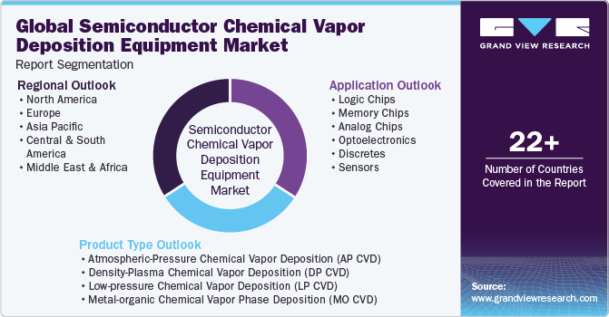
This report forecasts revenue growth at global, regional, and country levels and analyzes the latest industry trends and opportunities in each of the sub-segments from 2018 to 2030. For the purpose of this study, Grand View Research has segmented the semiconductor chemical vapor deposition equipment market report based on product type, application, and region:
-
Product Type Outlook (Revenue, USD Million, 2018 - 2030)
-
Atmospheric-Pressure Chemical Vapor Deposition (AP CVD)
-
Density-Plasma Chemical Vapor Deposition (DP CVD)
-
Low-pressure Chemical Vapor Deposition (LP CVD)
-
Metal-organic Chemical Vapor Phase Deposition (MO CVD)
-
-
Application Outlook (Revenue, USD Million, 2018 - 2030)
-
Logic Chips
-
Memory Chips
-
Analog Chips
-
Optoelectronics
-
Discretes
-
Sensors
-
-
Regional Outlook (Revenue, USD Million, 2018 - 2030)
-
North America
-
U.S.
-
Canada
-
Mexico
-
-
Europe
-
Germany
-
UK
-
France
-
Spain
-
Netherlands
-
Italy
-
-
Asia Pacific
-
China
-
Japan
-
India
-
South Korea
-
Malaysia
-
Taiwan
-
-
Central & South America
-
Middle East & Africa
-
Frequently Asked Questions About This Report
b. The global semiconductor chemical vapor deposition equipment market size was estimated at USD 4.5 billion in 2023 and is expected to reach USD 4.80 billion in 2024.
b. The semiconductor chemical vapor deposition equipment market, in terms of revenue, is expected to grow at a compound annual growth rate of 7.7% from 2024 to 2030 to reach USD 7.50 billion by 2030.
b. Asia Pacific dominated the global semiconductor chemical vapor deposition equipment market in terms of revenue, in 2023. The governments have played a pivotal role in the semiconductor industry in the region. As a result, a list of investments is in the pipeline. For instance, companies in Taiwan plan to invest over USD 107 billion in semiconductor production by 2025.
b. Some of the key players operating in the semiconductor chemical vapor deposition equipment market include Aixtron Se, Applied Materials, Inc., Asm International, Cvd Equipment Corporation, Oxford Instruments Plc, NBM Design., Blue Wave Semi, PhotonExport, Vivid Inc. among others.
b. The upsurge in the demand of microelectronic and semiconductor devices, technological advancements in the semiconductor industry, along with the rise in the usage of semiconductor materials in AI programs & AI driven electronics are some of the primary factors contributing to the market growth.
Share this report with your colleague or friend.
![gvr icn]()
NEED A CUSTOM REPORT?
We can customize every report - free of charge - including purchasing stand-alone sections or country-level reports, as well as offer affordable discounts for start-ups & universities. Contact us now
![Certified Icon]()
We are GDPR and CCPA compliant! Your transaction & personal information is safe and secure. For more details, please read our privacy policy.
We are committed towards customer satisfaction, and quality service.
"The quality of research they have done for us has been excellent."
