- Home
- »
- Next Generation Technologies
- »
-
Focused Ion Beam Market Size & Share Report 2026-2033GVR Report cover
![Focused Ion Beam Market (2026 - 2033)Report]()
Focused Ion Beam Market (2026 - 2033)
Size, Share & Trends Analysis Report By Type (Ga+ Liquid Metal, Gas Field, Plasma), By Application (Failure Analysis, Nanofabrication, Device Modification, Circuit Edit, Counterfeit Detection), By Vertical, By Region and Segment Forecasts
- Report Summary
- Table of Contents
- Segmentation
- Methodology
- Download FREE Sample
-
 Download Sample Report
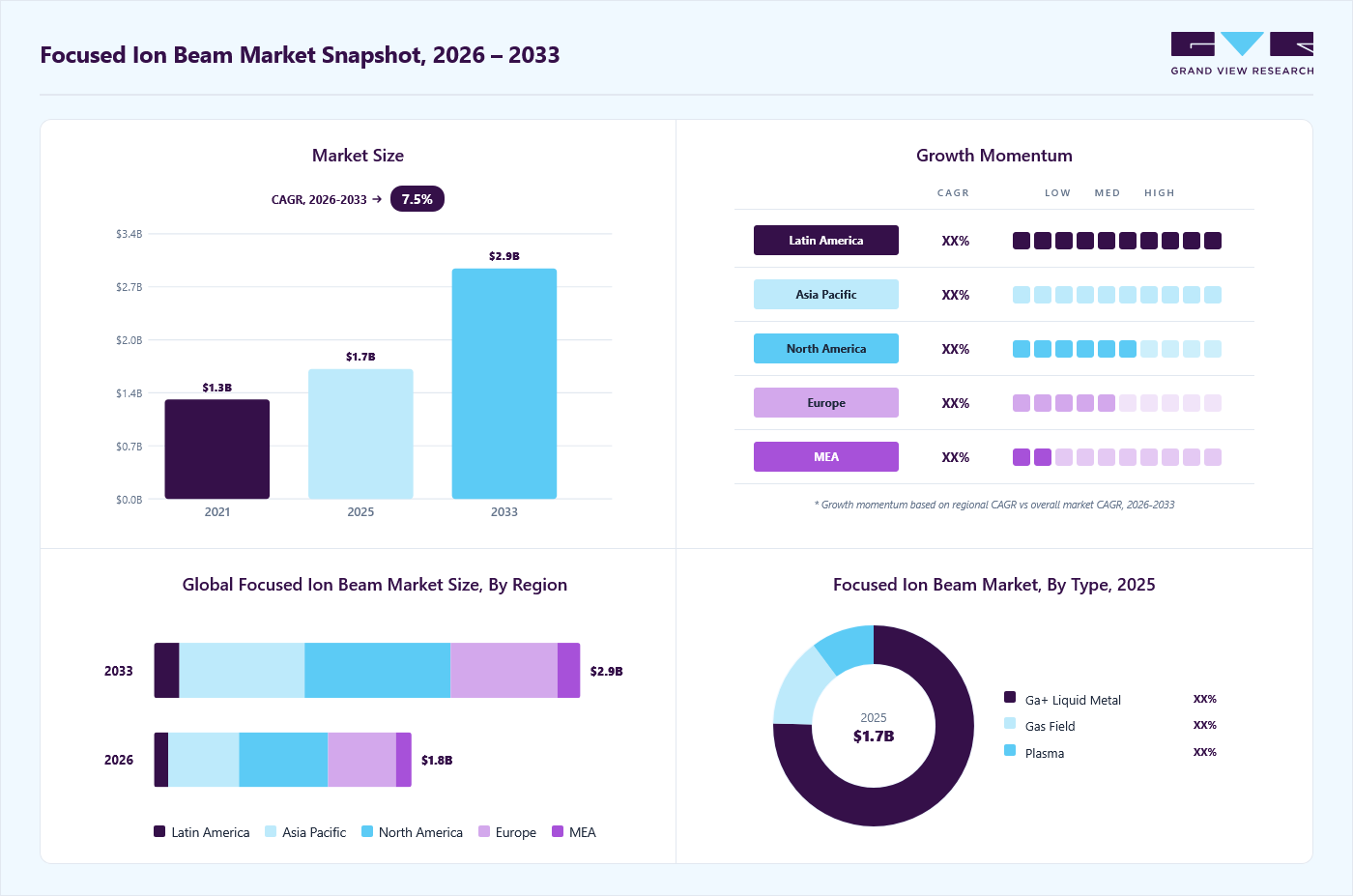
Market Size, 2025
$1.7BMarket Estimate, 2026
$1.8BMarket Forecast, 2033
$2.9BCAGR, 2026–2033
7.5%Focused Ion Beam Market Summary
The global focused ion beam market size was valued at USD 1.7 billion in 2025 and is projected to grow from USD 1.8 billion in 2026 to USD 2.9 billion by 2033, growing at a CAGR of 7.5% from 2026 to 2033. North America dominated the global market with the largest revenue share of 34.6% in 2025. The focused ion beam (FIB) market is primarily driven by increasing demand for precise material characterization, nanofabrication, and failure diagnostics across diverse industries.
Key Market Trends & Insights
- By type: Ga+ liquid metal led the market, holding the largest revenue share of 80.9% in 2025.
- By application: Failure analysis segment led the market, holding the largest revenue share of 31.8% in 2025.
- By vertical: Electronics & semiconductor segment held the highest market share of 48.6% in 2025.
Regional Highlights
- Largest regional market: North America (34.6% revenue share, 2025)
- Fastest-growing regional market: Asia Pacific (highest CAGR, 2026-2033)
- By country: The U.S. held the largest market share in 2025.
Market Size & Forecast
- Market size in 2025: USD 1.7 Billion
- Estimated market size in 2026: USD 1.8 Billion
- Projected market size by 2033: USD 2.9 Billion
- CAGR (2026-2033): 7.5%
The market is centered on tools that use a tightly focused beam of ions, commonly gallium, to image, modify, or analyze materials at micro- and nanoscale levels. These systems are essential in industries that require high precision, such as semiconductors, materials science, and life sciences. FIB systems can perform imaging, milling, deposition, and circuit editing, making them versatile instruments. They are often integrated with scanning electron microscopes to form dual-beam systems. This integration enhances analytical capabilities and broadens application scope. The market for FIB technology continues to grow due to demand for miniaturized and high-performance components. As nanofabrication and device complexity increase, FIB tools are becoming more indispensable in research and manufacturing environments.")
Growth in the semiconductor sector is one of the main market drivers. As electronic devices become smaller and more complex, precise tools such as FIBs are needed for inspection and modification. These systems are widely used for failure analysis, process development, and sample preparation. The market also benefits from increased research in nanotechnology and advanced materials. Life sciences applications, such as biological sample preparation, also contribute to demand. FIB’s ability to work with a variety of materials across sectors supports its expanding market base. The growing interest in high-resolution imaging and material characterization further fuels this demand.
Advancements also influence the automation of FIB systems, artificial intelligence, and the software integration market. These enhancements improve accuracy, ease of use, and efficiency in complex tasks. As a result, industries are adopting FIB tools for more sophisticated analyses and processes. Emerging applications in additive manufacturing and quantum research are expanding the technology’s reach. Collaborations between research institutions and commercial manufacturers are helping drive innovation. Together, these trends are shaping the future market landscape. Continuous R&D investments are expected to accelerate the development of the next-generation FIB system.
Market Dynamics
The global focused ion beam market is experiencing steady growth driven by increasing demand for semiconductor failure analysis and advanced materials research. Rising complexity in integrated circuits is increasing the need for precise nanoscale imaging and sample preparation technologies. The market is benefiting from growing investments in semiconductor manufacturing and process development activities. Demand from research institutions and nanotechnology applications is further supporting market expansion. Technological advancements are improving system accuracy, throughput, and automation capabilities.
The growing complexity of semiconductor devices is increasing the need for advanced failure analysis solutions. Modern chips incorporate smaller nodes, higher transistor densities, and more intricate architectures, making defect identification more challenging. Focused ion beam systems provide precise material removal and cross-sectioning capabilities for detailed examination of device structures. These systems enable engineers to identify the root causes of performance issues and manufacturing defects. Semiconductor manufacturers use FIB technology to improve process control and product quality. As demand for advanced chips continues to grow, the need for failure analysis tools is supporting expansion of the Focused Ion Beam market.
Defect inspection is becoming increasingly important as semiconductor manufacturers strive to maintain high production yields and device reliability. Even minor defects can affect the performance and functionality of advanced semiconductor components. Focused ion beam systems provide high-resolution imaging and nanoscale analysis capabilities for detailed defect investigation. The technology helps manufacturers detect, characterize, and address defects during different stages of the production process. This supports quality assurance efforts and reduces the risk of costly production losses. Growing emphasis on precision manufacturing is driving greater adoption of FIB systems for defect inspection applications.
Focused ion beam systems require substantial capital expenditure due to their advanced imaging, milling, and analytical capabilities. The sophisticated components and precision engineering involved in these instruments contribute to their premium pricing. Many research institutions, universities, and smaller organizations face challenges in allocating sufficient budgets for such equipment. Financial constraints can delay purchasing decisions and limit access to advanced characterization technologies. The impact is particularly evident in regions with lower levels of research funding and industrial investment. This pricing barrier restricts adoption across a broader range of potential users.
Beyond acquisition costs, these systems involve significant expenses throughout their operational lifecycle. Regular maintenance, calibration, and replacement of critical components add to ongoing expenditures. Organizations may also need dedicated infrastructure and controlled environments to ensure optimal system performance. These requirements increase the overall financial burden associated with system ownership. Budget limitations can affect the ability of users to expand or modernize their equipment base. Consequently, cost-related challenges continue to influence purchasing decisions across the market.
The semiconductor industry is increasingly adopting advanced packaging technologies to improve performance, power efficiency, and device integration. Approaches such as 2.5D packaging, 3D ICs, and chiplet-based architectures are becoming more common in high-performance computing, AI, and data center applications. These advanced structures involve complex interconnects and multilayer designs that require detailed inspection and characterization. Focused ion beam systems provide precise cross-sectioning and imaging capabilities for analyzing these intricate architectures. The technology helps engineers evaluate structural integrity and manufacturing quality. This trend is creating new growth opportunities for the focused ion beam market.
As advanced packaging becomes more widely implemented, manufacturers require sophisticated tools to support process development and quality control. Focused ion beam systems enable detailed investigation of packaging defects, interconnect reliability, and material interactions at the nanoscale level. These capabilities support optimization of manufacturing processes and product performance. Demand for advanced packaging solutions is increasing across consumer electronics, automotive, telecommunications, and data center applications. Continued innovation in semiconductor design is expected to drive further adoption of complex packaging architectures. This expanding application area is creating favorable conditions for growth in the Focused Ion Beam market.
Analyst Perspective
The Focused Ion Beam market is a specialized area driven by growing need for detailed semiconductor analysis and nanoscale material study. Demand is rising as chips and devices become more complex, especially with advanced packaging and precision manufacturing. A small group of established companies dominates the space because of high technical requirements and strong research capabilities. Continuous improvements in system performance and automation are helping vendors stand out from each other. The market is expected to grow steadily as industries rely more on advanced tools for analysis and fabrication.
Market Concentration & Characteristics
The focused ion beam market exhibits a concentrated competitive structure, with a limited number of established manufacturers accounting for a significant share of global revenue. High technological complexity and substantial research and development requirements create barriers to entry for new participants. The market is characterized by the presence of specialized companies with strong expertise in microscopy, semiconductor analysis, and nanotechnology instrumentation. Customers often prioritize system performance, precision, and technical support when selecting suppliers. Long product development cycles and high capital requirements further reinforce the positions of established vendors. These factors contribute to a market structure that is positioned toward concentration.

The market is characterized by a high degree of innovation driven by advancements in semiconductor manufacturing and materials research. Companies continuously enhance imaging resolution, automation capabilities, and analytical performance to address evolving customer requirements. Demand is concentrated among semiconductor manufacturers, research institutions, and advanced materials laboratories. Service substitution remains limited due to the unique capabilities of focused ion beam systems in nanoscale milling and characterization applications. Regulatory considerations, including export controls and technology compliance requirements, influence market operations in certain regions.
Type Insights
Based on type, the Ga+ Liquid Metal segment led the market with the largest revenue share of 80.9% in 2025. FIB systems have become widespread in various industries, such as electronics and semiconductors, for failure analysis, defect repair, and circuit editing. Furthermore, these systems have been employed in materials science research for microstructure analysis, composition analysis, and 3D imaging. The Ga+ liquid metal ion sources, characterized by high resolution and precision, play a crucial role in both fields. Its high accuracy and stability drive this segment, making it especially valuable in semiconductor failure analysis, circuit editing, and nanofabrication.
The plasma segment is expected to grow at the fastest CAGR over the forecast period. The plasma segment of FIB systems is driven by various ion species such as xenon, oxygen, argon, and nitrogen. These allow for flexible, site-specific, and high-volume material removal with enhanced sputtering efficiency and beam currents reaching up to 2.5 μA. Plasma FIBs deliver smoother cuts, minimize curtaining artifacts, and provide quicker access to target areas than conventional gallium FIBs, making them well-suited for high-throughput 3D imaging and large-area planar milling. The broader and more collimated plasma ion beam improves milling speed and surface quality, enabling advanced biological and materials science imaging applications.
Vertical Insights
Based on vertical, the electronics & semiconductor segment led the market with the largest revenue share of 48.6% in 2025. The market is driven by the need for precise circuit modification, defect analysis, and photomask repair as key processes in integrated circuit manufacturing and troubleshooting. FIB technology allows for nanoscale, site-specific milling and material deposition, enabling manufacturers to remove unwanted connections or add conductive paths to repair or improve semiconductor components. For instance, in March 2025, ZEISS introduced the Crossbeam 550 Samplefab, a next-generation FIB-SEM system to transform TEM sample preparation in the electronics and semiconductors. Featuring automation, the system can prepare up to 10 lamellae in less than eight hours without manual intervention, achieving thinning down to 100 nm on a wide range of semiconductors, establishing a new standard for efficiency and reliability in semiconductor analysis.
The bioscience segment is anticipated to grow at the fastest CAGR during the forecast period. The growing demand includes the growing need for high-resolution imaging and precise sample preparation in biological research, especially in areas like cryo-electron microscopy and structural biology. FIB technology allows for nanoscale milling and 3D tomography of biological samples while preserving their native structures, offering valuable insights into microorganisms, viruses, and cellular components. Innovations such as cryo-plasma FIB milling minimize sample damage even at higher ion currents, enabling detailed in situ analysis. Integrating AI and automation further improves precision and throughput, broadening the use of FIB in biomedical research and biomaterials development.
Application Insights
Based on application, the failure analysis segment led the market with the largest revenue share of 31.8% in 2025. The market is growing due to the offering nature for unmatched precision in nanoscale material removal and imaging. They facilitate accurate inspection, cross-sectioning, and defect analysis, which are vital for the semiconductor and microelectronics industries. Adopting advanced gallium and plasma FIB technologies, AI-driven automation, and machine learning improves milling efficiency, beam consistency, and real-time defect detection. This combination of accuracy and adaptability makes FIB an essential tool for high-resolution failure analysis, circuit editing, and nanoscale material modification.

The device modification segment is anticipated to grow at the fastest CAGR during the forecast period. The device modification market is driven by its essential role in semiconductor manufacturing, especially for circuit edits, defect analysis, and photomask repair. FIB systems offer precise, site-specific milling and depositing using a focused ion beam, most often gallium ions, enabling nanoscale material removal and deposition. Combining in situ imaging and sectioning with gas-assisted etching or deposition improves accuracy and efficiency. Furthermore, integrating FIB with scanning electron microscopy (SEM) in dual-beam setups enhances detailed inspection and device modification, fueling demand in advanced semiconductor development and research.
Regional Insights
North America dominated the focused ion beam market with the largest revenue share of 34.6% in 2025. Advancements in semiconductor manufacturing, materials science, and nanotechnology drive the market. The U.S. is at the forefront, with continuous investments in cutting-edge FIB technologies for applications ranging from failure analysis in semiconductors to advanced materials characterization in aerospace and defense. The region's robust ecosystem, comprising leading FIB system manufacturers and research institutions, further propels market expansion.

U.S. Focused Ion Beam Market Trends
The Focused Ion Beam market in the U.S. held the largest share in the North America region in 2025, driven by advancements in semiconductor manufacturing, materials science, and nanotechnology. FIB systems are increasingly utilized for applications such as failure analysis, nanofabrication, and device modification within the electronics and semiconductor sectors. Major U.S. companies like Thermo Fisher Scientific and Veeco Instruments are at the forefront of FIB technology, catering to diverse industries including aerospace, defense, and life sciences.
Europe Focused Ion Beam Market Trends
The focused ion beam market in Europe is expected to grow significantly over the forecast period. This market is driven primarily by the increasing demand for semiconductors and materials science. European research institutions and advanced manufacturing facilities are investing in FIB systems to support nanotechnology, failure analysis, and sample preparation for transmission electron microscopy. Countries like Germany, the Netherlands, and France are leading in adoption due to their strong semiconductor ecosystems and emphasis on R&D.
Asia Pacific Focused Ion Beam Market Trends
The focused ion beam market in Asia Pacific is anticipated to register the fastest CAGR over the forecast period. The Asia Pacific region is witnessing a notable surge in the adoption of FIB technology, driven by advancements in semiconductor manufacturing, materials science, and nanotechnology. China, Japan, and South Korea are at the forefront, leveraging FIB systems for precise failure analysis, device modification, and nanofabrication in their robust electronics and semiconductor sectors.
Key Focused Ion Beam Company Insights
Some key companies in the FIB industry are Thermo Fisher Scientific, Zeiss, and Hitachi High-Technologies Corporation.
-
Thermo Fisher Scientific is a prominent player in the Focused Ion Beams (FIB) market, offering advanced solutions through its electron microscopy and FIB systems. The company supports various applications, including semiconductor failure analysis, materials science, and life sciences. Its FIB technology is integrated into dual-beam platforms, enhancing precision and enabling nanoscale imaging and sample preparation.
-
Zeiss is a German manufacturer renowned for its optical systems and optoelectronics, including advanced microscopy solutions. It is a key electron and ion microscope market player, offering high-resolution imaging and analytical capabilities. Zeiss develops and supplies state-of-the-art FIB-SEM systems, essential for precise material modification and 3D characterization at the nanoscale. Its focus on innovative optical design extends to providing solutions for demanding semiconductor and materials research applications.
Key Focused Ion Beam Companies:
The following key companies have been profiled for this study on the focused ion beam market.
-
Thermo Fisher Scientific
-
Zeiss
-
Hitachi High-Technologies Corporation
-
JEOL Ltd.
-
TESCAN GROUP, a.s.
-
Fibics Incorporated
-
Raith GmbH
-
FOCUS GmbH
-
A&D Company, Limited
-
Veeco Instruments, Inc.
-
Eurofins Scientific
-
Delong Instruments Co., Ltd.
Competitive Benchmarking
Category
Operating Strategies
Competitive Edge
Weakness
Established Players (Thermo Fisher Scientific, Carl Zeiss AG, Hitachi High-Technologies Corporation, JEOL Ltd.)
- Matured players focus on advanced integrated systems, strong R&D capabilities, global reach, and long-term service partnerships with semiconductor and research customers.
- Strong brand reputation, advanced technology portfolios, global presence, and established service networks support their market position.
- High system cost, longer product development cycles, and limited flexibility in highly customized or niche applications can restrict adaptability.
Emerging Players (Fibics Incorporated, Veeco Instruments Inc., Eurofins Scientific)
- Emerging and niche players focus on specialized applications, flexible offerings, and cost-effective or service-based models, targeting niche or regional demand.
- Specialized offerings, cost efficiency, flexibility, and focus on niche or underserved applications support their competitiveness.
- Limited global reach, weaker brand recognition, and constrained R&D resources can reduce competitiveness against established players.
Recent Developments
-
In April 2025, ZEISS announced the launch of ZEN core, a versatile and efficient software suite designed to operate the full range of ZEISS scanning electron microscopes (SEMs), including focused ion beam scanning electron microscopes (FIB-SEMs). This integrated platform enhances user experience by providing streamlined control, advanced imaging capabilities, and automation features across multiple instrument types.
-
In April 2025, ZEISS Medical Technology received 510(k) clearance from the U.S. Food and Drug Administration (FDA) for the INTRABEAM 700 system. This advanced platform delivers robotic-assisted precision to facilitate intraoperative radiation therapy (IORT), enhancing treatment accuracy in neuro-oncology and breast cancer care. Featuring a modern digital-first architecture, the INTRABEAM 700 streamlines clinical workflows through SMART efficiency and seamless connectivity, thereby improving operational integration and patient outcomes in surgical oncology settings.
-
In January 2025, JEOL USA announced the launch of its new broad ion beam milling instruments, the Cross Section Polisher and the Cooling Cross Section Polisher. These advanced tools are designed to produce high-quality, artifact-free cross sections, optimized for imaging and microanalysis using scanning electron microscopy (SEM), electron probe microanalysis (EPMA), and Auger electron spectroscopy. Introducing these instruments enhances sample preparation capabilities, enabling more precise and reliable materials characterization across various research and industrial applications.
Focused Ion Beam Market Report Scope
Report Attribute
Details
Market size in 2025
USD 1.7 billion
Estimated market size in 2026
USD 1.8 billion
Projected market size by 2033
USD 2.9 billion
Growth rate
CAGR of 7.5% from 2026 to 2033
Base year for estimation
2025
Historical data
2021 - 2024
Forecast period
2026 - 2033
Quantitative units
Revenue in USD million/billion and CAGR from 2026 to 2033
Report coverage
Revenue forecast, company ranking, competitive landscape, growth factors, and trends
Segments covered
Type, application, vertical, region
Regional scope
North America; Europe; Asia Pacific; Latin America; MEA
Country scope
U.S.; Canada; Mexico; Germany; UK; France; China; Japan; India; Australia; South Korea; Brazil; KSA; UAE; South Africa
Key companies profiled
Thermo Fisher Scientific; Zeiss; Hitachi High-Technologies Corporation; JEOL Ltd.; TESCAN GROUP, a.s.; Fibics Incorporated; Raith GmbH; FOCUS GmbH; A&D Company, Limited; Veeco Instruments, Inc.; Eurofins Scientific; Delong Instruments Co., Ltd.
Customization scope
Free report customization (equivalent up to 8 analysts' working days) with purchase. Addition or alteration to country, regional & segment scope.
Pricing and purchase options
Avail customized purchase options to meet your exact research needs. Explore purchase options
Global Focused Ion Beam Market Report Segmentation
This report forecasts revenue growth at the global, regional, and country levels and provides an analysis of the latest industry trends in each of the sub-segments from 2021 to 2033. For this study, Grand View Research has segmented the global focused ion beam market report based on type, application, vertical, and region:

-
Type Outlook (Revenue, USD Million, 2021 - 2033)
-
Ga+ Liquid Metal
-
Gas Field
-
Plasma
-
-
Application Outlook (Revenue, USD Million, 2021 - 2033)
-
Failure Analysis
-
Nanofabrication
-
Device Modification
-
Circuit Edit
-
Counterfeit Detection
-
-
Vertical Outlook (Revenue, USD Million, 2021 - 2033)
-
Electronics & Semiconductor
-
Industrial Science
-
Bioscience
-
Material Science
-
-
Regional Outlook (Revenue, USD Million, 2021 - 2033)
-
North America
-
U.S.
-
Canada
-
Mexico
-
-
Europe
-
Germany
-
UK
-
France
-
-
Asia Pacific
-
China
-
Japan
-
India
-
South Korea
-
Australia
-
-
Latin America
-
Brazil
-
-
Middle East and Africa (MEA)
-
UAE
-
KSA
-
South Africa
-
-
Research Methodology
Segment Definition
Segment -Type
Revenue capture definition
Ga+ Liquid Metal
In Ga+ liquid metal-based systems, revenue is generated through applications such as high-precision imaging, circuit editing, and failure analysis, where gallium ion sources enable accurate nanoscale material processing. These systems are widely adopted in semiconductor and materials research environments that require fine structural control.
Gas Field
Gas field ion source systems generate revenue through ultra-high-resolution imaging and detailed nanoscale characterization applications. They are primarily used in advanced research settings where precise surface and atomic-level analysis is required for material evaluation.
Plasma
Plasma-based systems generate revenue through high-throughput material removal, large-area milling, and efficient sample preparation workflows. These systems are increasingly deployed in semiconductor manufacturing and industrial research where faster processing and broader application coverage are required.
Segment - Application
Revenue capture definition
Failure Analysis
Focused ion beam systems generate revenue through detailed examination of defects within semiconductor devices and advanced materials. These systems are used to pinpoint root causes of performance issues and improve manufacturing reliability.
Nanofabrication
Revenue is generated when focused ion beam technology is used to create and manipulate structures at the nanoscale. It supports precise patterning and material modification for advanced research and device development.
Device Modification
In device modification applications, revenue is derived from nanoscale adjustments made to improve or alter the performance of semiconductor components. These systems enable controlled changes in material structures for experimental and production purposes.
Circuit Edit
Revenue comes from the ability of focused ion beam systems to repair, modify, or fine-tune integrated circuits after fabrication. This capability is essential for debugging and optimizing semiconductor designs.
Counterfeit Detection
Focused ion beam systems support revenue generation by enabling internal inspection of electronic components to verify authenticity. This helps identify counterfeit or substandard devices within supply chains.
Segment - Vertical
Revenue capture definition
Electronics & Semiconductor
Focused ion beam systems generate revenue in electronics and semiconductor applications through precise failure analysis, circuit editing, and device inspection. These capabilities support chip development, validation, and manufacturing optimization.
Industrial Science
In industrial science, revenue is generated through material inspection, surface analysis, and structural evaluation of engineered components. These systems are used to improve product quality, durability, and process efficiency.
Bioscience
Revenue is captured in bioscience applications where focused ion beam systems assist in high-resolution imaging and sample preparation for biological structures. They support advanced research in cellular and molecular-level analysis.
Material Science
Material science applications generate revenue through nanoscale characterization and modification of advanced materials. These systems help researchers study composition, structure, and behavior under different conditions.
Estimation Model
Demand Generation Layer
Technology Availability Layer
Deployment & Adoption Layer
Market Value Layer
What drive is Focused Ion Beam (FIB) demand?
Which Focused Ion Beam technology are available ?
How is Focused Ion Beam adopted ?
How is Focused Ion Beam market value generated?
Industries such as semiconductors, electronics, materials science, nanotechnology, and life sciences drive demand for FIB systems through increasing need for nanoscale imaging, failure analysis, and precision material modification.
Availability of Ga-liquid metal ion sources, plasma FIB systems, gas field ion sources, and integrated dual-beam platforms determines the range of applications across imaging, milling, and circuit editing workflows.
FIB adoption varies across applications such as semiconductor failure analysis, nanofabrication, device modification, circuit editing, and counterfeit detection depending on system cost, complexity, and end-user maturity.
Market value is derived from revenues generated through system sales, service contracts, software integration, and upgrades across semiconductor manufacturers, research institutes, and advanced materials laboratories globally.
Delivered Customizations
This report has been delivered with the following In-depth customizations
Client Request
Customization Delivered
Value Adds
Technology & Innovation Assessment
Emerging technology mapping, innovation pipeline tracking, and adoption readiness analysis focused on beam systems across semiconductor and materials research applications.
Identified future technology directions, supported R&D prioritization, and evaluated commercialization potential of advanced ion beam solutions.
Product Positioning & Competitive Intelligence
Detailed benchmarking focused on ion beam systems, including feature comparison, pricing structures, and competitor strategy evaluation.
Strengthened differentiation strategy, supported pricing optimization, and highlighted gaps in competitor offerings and customer requirements.
Market Entry & Expansion Assessment
Regional demand sizing, customer segmentation, competitive landscape mapping, and regulatory environment assessment for key geographies.
Identified high-growth opportunities, supported go-to-market strategy development, and enabled risk-aware expansion planning.
Frequently Asked Questions About This Report
Asia Pacific is the fastest-growing region over the forecast period.
The Ga+ Liquid Metal segment led with a 80.9% revenue share in 2025 and is expected to be the fastest-growing segment during the forecast period.
The Failure Analysis segment led with 31.8% revenue share in 2025, while Device Modification is the fastest-growing segment.
Some key players operating in the focused ion beam market include Thermo Fisher Scientific; Zeiss; Hitachi High–Technologies Corporation; JEOL Ltd.; TESCAN ORSAY HOLDING, a.s.; Fibics Incorporated; Raith GmbH; Focus GmbH; A&D Company; Veeco Instruments, Inc.; Eurofins Scientific; Delong Instruments Co., Ltd.
Factors such as the increasing demand for high–resolution microscopy and the rising investment in research and development activities are driving the growth of the focused ion beam market
The global focused ion beam market size was estimated at USD 1.7 billion in 2025 and is expected to reach USD 1.8 billion in 2026.
The global focused ion beam market is expected to grow at a compound annual growth rate of 7.5% from 2026 to 2033, reaching USD 2.9 billion by 2033
North America dominated the focused ion beam market with a revenue share of 34.6% in 2025. Regional growth is attributed to the rapidly growing semiconductor industry, with North America emerging as a hub for semiconductor manufacturing
The Electronics & Semiconductor segment led with a 48.6% revenue share in 2025, while Bioscience is the fastest-growing segment.
About the Author(s)
Next Generation Technologies Research Team
Technology · Next Generation TechnologiesThis report was authored by the next generation technologies research team at Grand View Research - comprising two research analysts, one senior research analyst, and one industry expert - with specialized expertise in the next generation technologies segment of the technology industry. All findings are based on proprietary technology databases, executive interviews, and regulatory analysis, subject to internal peer review prior to publication.
Last Updated:
Speak to Analyst


Share this report with your colleague or friend.
Need a Tailored Report?
Customize this report to your needs — add regions, segments, or data points, with 20% free customization.

ISO 9001:2015 & 27001:2022 Certified
We are GDPR and CCPA compliant! Your transaction & personal information is safe and secure. For more details, please read our privacy policy.